
301 Moved Permanently
The collapse of PV prices severely changed the manufacturing landscape, shifting the vast majority of the world’s silicon wafer and cell production to China and creating something of a commodity market. In this environment, research and development of more efficient modules was overshadowed by oversupply. Many manufacturers found it impossible to compete on the basis of module performance, where incremental increases in module efficiencies required significant investment and modules deemed “good enough” were readily at hand.
Nevertheless, some PV technology developers continued to hone their machines and their processes, if only in the research laboratory.
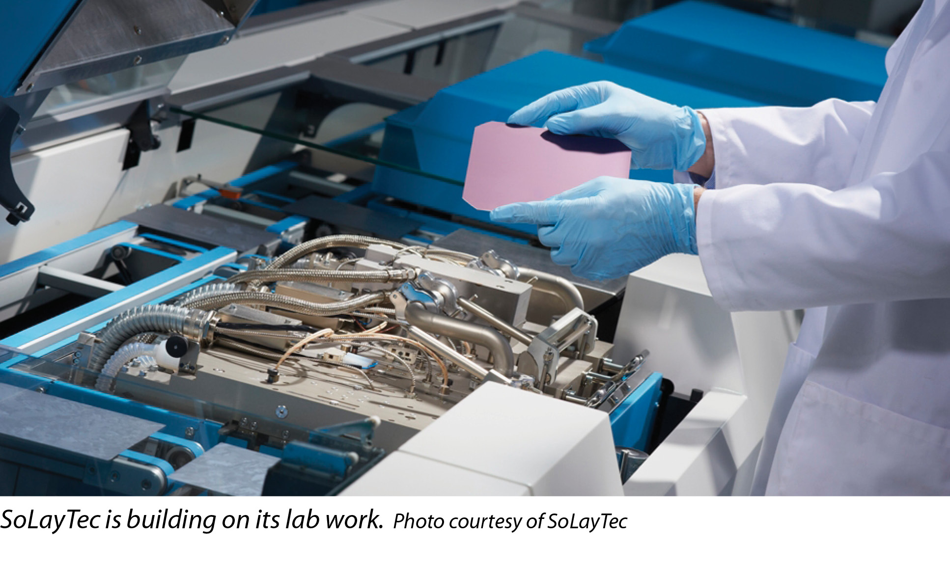
Netherlands-based SoLayTec began as a spin-off from the Toegepast Natuurwetenschappelijk Onderzoek research organization to pursue the development of a new process for improving efficiencies in PV cells. The company specializes in spatial atomic layer deposition (ALD) technology for aluminum oxide (Al2O3) passivation layers on solar cells. In a nutshell, the ALD machines apply a 5 nanometer-thin Al2O3 layer on passivated-emitter rear-contact (PERC) solar cells. SoLayTec and its research partners have reported achieving a conversion efficiency of 20.1% using this technique.
“All cell manufacturers need to improve their cell efficiency to stay competitive,” says Roger Görtzen, SoLayTec’s co-founder and manager of sales and marketing. “Most techniques focus on improving the properties of the front side of the wafer. Our Al2O3 passivation technique is a way to improve the back side as well.”
According to Görtzen, the company’s early work involved developing ALD equipment for other research institutions, such as imec, the Institute for Solar Energy Research, Fraunhofer ISE and the Solar Energy Research Institute of Singapore. Working with RENA, a Germany-based supplier of PV wet processing solutions and equipment, SoLayTec developed the InPassion LAB system. While the company still supports its research partners, it is now building production-scale machines for cell production lines. One of the main challenges in scaling the ALD technology up for production volumes was engineering effective process control for the precision work.
“In our reactor, we are moving wafers on air cushions without carriers,” Görtzen says. Among the benefits of eliminating carriers, he says, is that automation for loading and unloading the carriers can be eliminated. Plus, there are no carriers to heat or clean. “The wafers float on air, like a hovercraft, and we are shuttling them from left to right and backwards with max speeds of about 1.2 meters per second.”
Görtzen says the most challenging aspect of scaling the InPassion ALD production machine up from a process control perspective was not just improving gross output but reducing yield loss to breakage to make net output economically viable. The solution was to incorporate six deposition chambers that can be independently operated. If breakage occurs in one, the operator can clean it out while the others continue functioning.
Also, the Al2O3 layer is essentially invisible to the human eye. Moreover, a reliable in-line thickness measurement on such surface is almost impossible due to the surface roughness. Such verification must occur at process speeds in about 2 seconds per wafer. To accomplish this, the machine continuously measures all of the operating conditions relevant to the ALD process, Görtzen explains. The machine controls the temperature of all reactors, the amount of precursors, pressure for all chambers, wafer speed and movement, etc. If one of the controlled values is not within its threshold, the wafer is transferred to a reject bin. At the same moment, an operator is notified to take corrective action.
In December, SoLayTec sold its InPassion ALD machine to a tier-one Chinese PV manufacturer that had previously procured an InPassion LAB machine for research and development purposes. Ultimately, the manufacturer is expected to transition to mass-production of PV wafers based on PERC cells.
SoLayTec is not alone in its efforts to apply ALD techniques to PV manufacturing. South Korea-based AVACO, a maker of physical vapor deposition equipment, has developed a horizontal in-line modular ALD system for solar cell and other large-substrate processes. The company says its ALD system for large substrates can provide enhanced solar cell energy conversion efficiency through its buffer-layer deposition process. The first machines were shipped to a research and development facility in Asia this year.
The race to achieve higher efficiency solar cells is proceeding along many lines. In November, Sweden-based Midsummer, a supplier of production lines for manufacturing of flexible thin-film copper indium gallium di-selenide solar cells, introduced a high-speed process for manufacturing such cells that uses sputtering for all layers in the solar cell structure. Midsummer says it has achieved 15% active area efficiency on an entire 225 square-centimeter solar cell using its DUO machine employing this technology.
Sven Lindström, CEO of Midsummer, says the process works for stainless steel substrates that are suitable for flexible modules. He says stainless steel substrates are suitable not only for regular solar panels, but also for flexible, lightweight panels that can be used on membrane roofs, landfills or other structures where traditional glass modules cannot be applied.
In June, Fraunhofer ISE embarked on a partnership with Austria-based EV Group to develop equipment and process technology to enable electrically conductive and optically transparent direct-wafer bonds at room temperature. Fraunhofer ISE says direct-wafer bonding provides the ability to combine a variety of materials with optimal properties for integration into multi-junction solar cells. The new manufacturing processes are intended to enable mismatched material combinations.
The research institute expects direct-wafer bonding to play an important role in the development of next-generation III-V solar cell devices with applications in space, as well as in terrestrial concentrator photovoltaics.
Higher module efficiencies promise better yields, more productive use of available space and greater solar asset value over the long term. These trends are opening the doors to new manufacturing processes and putting to work concepts once relegated to laboratories. S
Process: Process Control
New Processes In PV Manufacturing Open Doors To Higher Efficiency
By Michael Puttré
As PV manufacturers strive to compete on solar yields, laboratory processes are moving into factories.
si body si body i si body bi si body b
si depbio
- si bullets
si sh
si subhead
pullquote
si first graph
si sh no rule
si last graph