
301 Moved Permanently
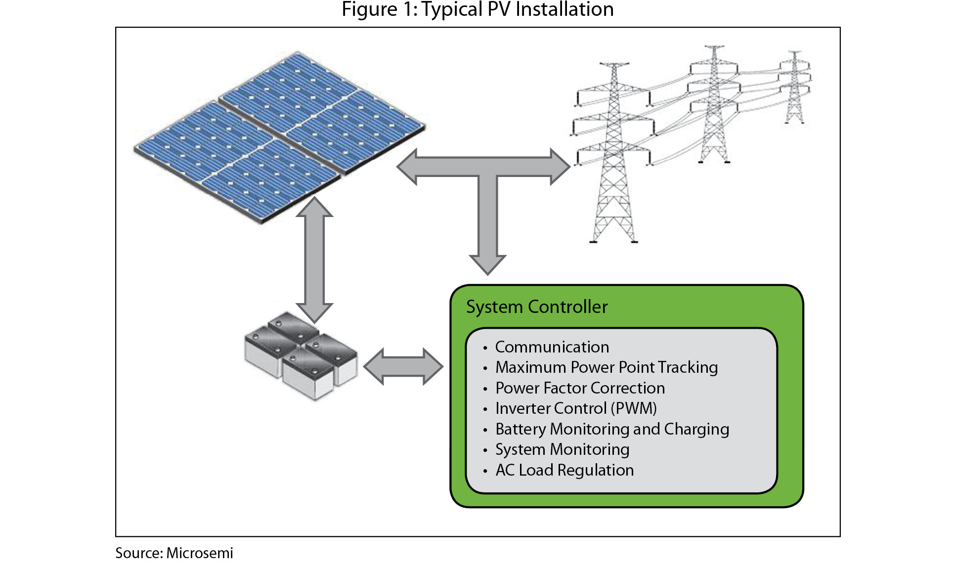
Photovoltaic inverter systems typically have two major sub-components: a controller used to implement system management tasks and control algorithms, and the AC-to-DC conversion circuit. The specifics of the controller depend on the type and configuration of the PV system as well as its functional requirements. Typical responsibilities include the following:
- grid and system monitoring;
- synchronization of the system with utility power for grid-connected systems;
- output power quality monitor-
ing; - protective functions for safety and compliance with standards and regulations;
- data logging, firmware updates and communications with the system operator;
- battery charge control - in the case of standalone systems, when the PV power produced exceeds the load demand, the controller prolongs the battery life by using a number of techniques to prevent over-charging; and
- smart metering used for grid-connected PV systems (in applications where utility power can be provided when demand exceeds solar electric power production, and credits can be given for any excess power when PV power production exceeds demand).
An additional controller responsibility is executing control and energy management algorithms that, in addition to being computationally demanding, can also have a significant effect on power efficiency.
The second major component, the DC-to-AC conversion circuit, converts DC power from the panels into AC power consistent with the voltage and power quality requirements of the utility grid. This conversion is accomplished by using a set of switching power devices such as metal oxide semiconductor field effect transistors (MOSFETs) or insulated gate bipolar transistors (IGBTs). The inverter circuit also includes active filtering circuitry to reduce the distortion caused by harmonics resulting from high-frequency switching.
There are several possible PV conversion circuit configurations. The choice is dictated by the number of power processing stages, the type of power decoupling, the types of interconnections between the stages and the type of the grid interface.
The efficiency of the conversion circuit is crucial in harvesting solar energy. Its efficiency depends on the topology used and the type of components and their operational characteristics (e.g., semiconductor switching devices, magnetic elements and capacitors).
HERIC and multilevel
Two inverter topologies have achieved higher efficiencies for grid-connected centralized inverters than alternatives. The first is the highly efficient and reliable inverter concept (HERIC), which incorporates an extra switch and diode pairs at the output to reduce losses by decoupling the output inductor from the input capacitor.
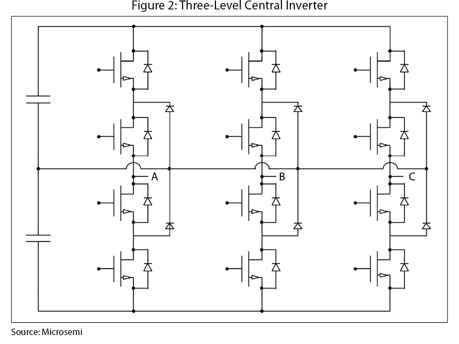
The second is the more complex multilevel inverter, whose most important difference is that each switch has only 50% of the voltage stress as compared to a HERIC topology. This reduction means that devices with much lower voltage can be used, leading to higher efficiency and lower device costs.
Further, the size of the electromagnetic interference (EMI) level and output filter (for cleaning the harmonics) can be reduced, thus lowering the overall cost of the system.
In addition to an inverter, a PV system can also have a DC-to-DC conversion stage. Although the DC-to-DC stage can be used to maintain the input voltage at the inverter at a constant and controlled level, as well as decouple the control of voltage and power, it can have a negative effect on system efficiency.
Other ways to improve efficiency are also now possible. For instance, silicon carbide (SiC) power transistors, which have recently become a reality, offer several advantages over traditional silicon or even gallium arsenide (GaAs) solutions, allowing for much greater power handling and higher switching rates.
There are projects underway to develop utility-grade devices, with an eye toward creating solid-state power transformers and high-power inverters for large-scale solar farms.
Another way to improve PV system efficiency is to use maximum power point tracking (MPPT) algorithms. MPPT enhances the PV system’s ability to control the power inverter so that it can react to changes in operating conditions.
As conditions change, MPPT algorithms maintain the optimum operating point by regulating the PV output for maximum power delivery. They also guarantee that the inverter does not draw more than the maximum PV array output power, thus preventing inverter collapse. An MPPT algorithm is typically deployed in the main controller; however, in certain cases where the operating conditions for individual PV modules differ significantly, it is more efficient to deploy the algorithm in the individual PV modules, allowing each to track independently.
This finer control over power conversion can greatly enhance the efficiency of the conversion process in applications using a larger number of modules. There are several possible algorithms for MPPT, each with its own advantages and disadvantages.
Efficiency also can be improved by using pulse width modulation (PWM) technology to control power switching components in the inverter circuit during DC-to-AC conversion. A PWM algorithm controls the switching component’s states in order to meet the time-average value of the voltage command.
Such algorithms can reduce losses in the inverter while optimizing the voltage utilization of the DC bus. PWM techniques have the advantage of being well understood and easy to implement in either hardware or software.
Finally, efficiency can be improved using power factor correction (PFC), which refers to the ratio of real power to reactive power, where real power is useful, and reactive power is wasted (the result of current and voltage being out of phase). Capacitive and inductive loads cause a poor power factor.
With a power factor of one, the voltage and current are in phase, providing maximum power. In effect, actively correcting the power factor improves system efficiency and is often required to meet certain energy efficiency standards.
PV inverters have traditionally been implemented using a variety of processors, including microcontrollers and digital signal processors (DSPs). A third option is to include programmable logic in the solution using field programmable gate array (FPGA) technology.
FPGA-based customized controllers take advantage of ongoing gains in FPGA technology, including cost improvements, higher performance, increased programming flexibility and increased gate capacity. They can now outperform microcontrollers, DSPs and application-specific integrated circuits in the equivalent price range.
DSPs have an advantage when implementing common DSP tasks. But when the design calls for highly optimized solutions with special functions such as PWM, MPPT and PFC algorithms, FPGAs provide a very low-cost hardware and software customization platform. For even greater flexibility, flash-based FPGAs offer the ability to be reprogrammed at any time, which reduces development costs while allowing for field upgrades and bug fixes. 
Reducing wires
The design and performance of a PV inverter system can be further enhanced by using a customizable system-on-chip (cSoC) platform that combines programmable logic with an embedded controller and configurable analog. The integration of board-level components into a single monolithic integrated circuit offers advantages including reduced cost and power dissipation, and shorter circuit delays due to the absence of board-level wiring.
By omitting the long wires needed to connect devices on the board, designers can also avoid other problems, such as parasitic ringing and oscillations.
The cSoC technology allows designers to choose where and how best to implement control functions (in hardware or software, or in a combination of the two). Additionally, the cSoC’s programmable analog can be used for critical tasks related to monitoring and evaluating operating conditions so that end-users and utilities have visibility into potential failures prior to their occurrence and can act accordingly.
Finally, the cSoC’s programmable fabric increases computational throughput by using hardware acceleration techniques to implement any needed DSP functions that cannot be feasibly implemented in the embedded microcontroller. In essence, arithmetic co-processing is accomplished through the highly parallel nature of an FPGA fabric.
Signal processing tasks are central to much of the control of advanced PV inverters. Although a microcontroller could host the signal processing algorithm, any need for performance will quickly outstrip the microprocessor’s bandwidth; moreover, the signal processing algorithm will compete with the host application for processor resources.
In contrast, the cSoC approach implements the required DSP functionality in hardware. Each time a signal processing function is needed, the embedded microprocessor makes calls to a coprocessor that has been constructed in the cSoC’s programmable logic core. This method unburdens the microprocessor while achieving the needed throughput. A number of off-the-shelf semiconductor intellectual property cores are available that greatly simplify the task of implementing DSP algorithms in hardware for PV system applications. S
Product: Utility/Large-Scale Inverters
Solar Inverter Components Can Raise Efficiencies
By Rufino Olay
A closer look at large-scale solar inverter topologies reveals that certain types of devices can improve plant operations.