
301 Moved Permanently
Arguably, the most important feature of a crystalline silicon photovoltaic cell involves its p-n junction. While most other cell properties mainly influence conversion efficiency, the p-n junction provides the basic function of the cell.
At this interface of p- and n-conductive semiconductors, electric charge carriers are generated by incoming light and separated according to their negative or positive charge, thus making current and voltage collection possible.
The overwhelming majority of today’s mass-manufactured solar cells use p-doped silicon wafers. This base material is typically composed of p-dopant boron. During cell processing, the introduction of n-doping phosphorus into the silicon wafer surface facing the sun forms the cell emitter.
The concentration of phosphorus in the emitter must be chosen to overcome the boron-doped base, thus creating the p-n junction. Junction or emitter depth ranges from 0.2 to 1 µm, according to process settings.
Several technologies are available to create the emitter, but ion implantation and plasma-enhanced chemical vapor deposition (PECVD) are used only in relatively small volume compared to the more widespread technology - thermal diffusion.
Thermal diffusion involves two separate steps to introduce dopant atoms into the wafer. First, wafers are coated with a dopant source. This step can be achieved using screen printing, a spray or different chemical vapor deposition processes. Second, the wafers are heated between 800° C and 900° C, which causes dopant atoms to diffuse into the wafer.
Diffusion steps
The most common technology employed for emitter creation involves the thermal diffusion of phosphorus atoms from phosphorus silicate glass (PSG). The process uses a batch furnace where 400 to 1,000 cells are doped simultaneously.
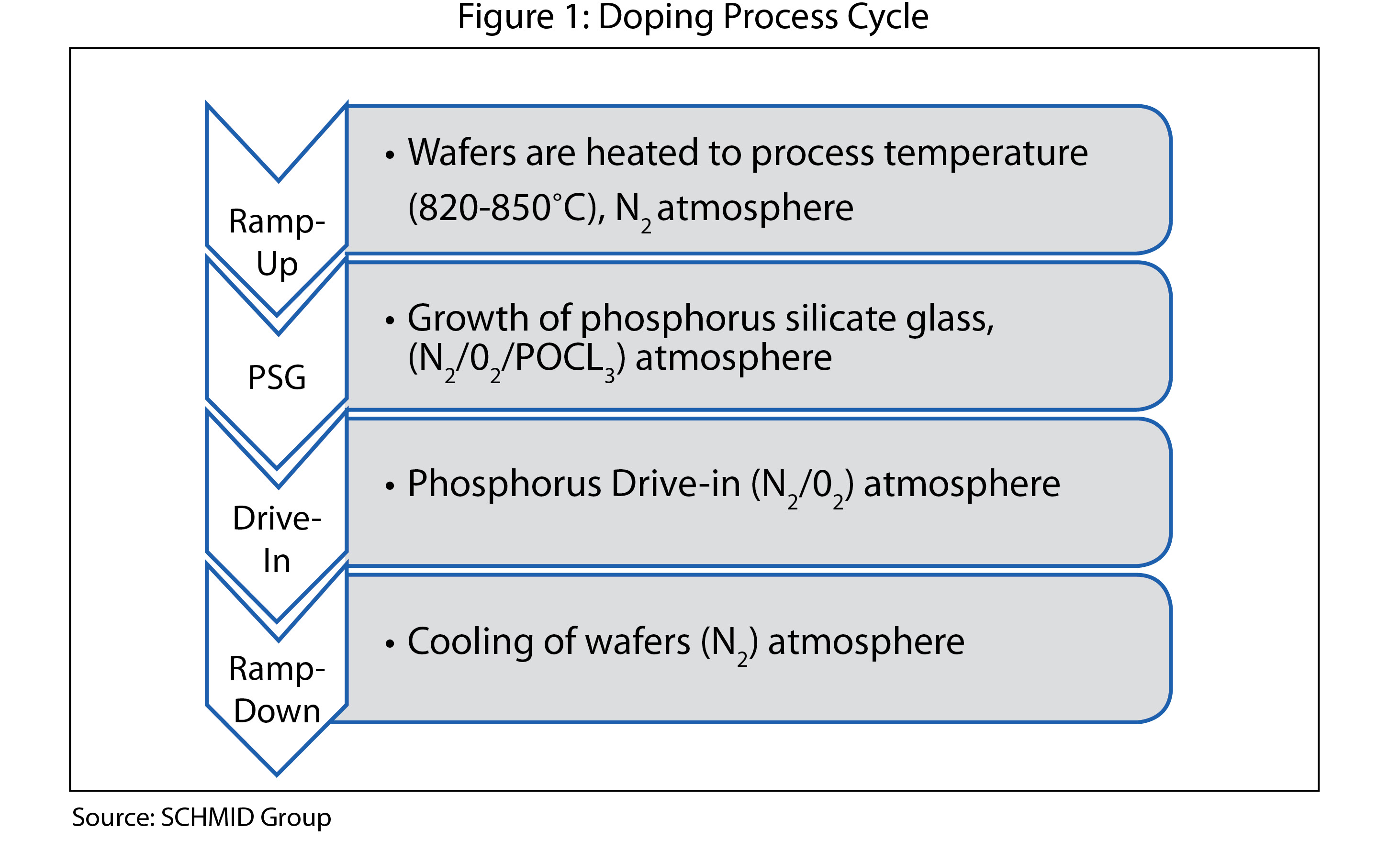
Wafers are exposed to a controlled atmosphere of nitrogen and oxygen at a temperature of approximately 820° C to 860° C. This leads to the growth of a thin layer of silica (SiO2). In addition, phosphorus oxychloride (POCl3) is injected into the process atmosphere.
POCl3 dissociates and reacts with oxygen, leading to the formation of chlorine gas (Cl2) and phosphorus oxide (P2O5). Chlorine gas readily reacts with most metals and, thus, cleanses wafer surfaces of metallic impurities that would otherwise negatively affect p-n junction quality.
At the same time, P2O5 dissolves into the silica, creating the dopant source PSG. Phosphorus atoms from the PSG diffuse into the wafer. This step, called “drive in,” will sometimes be carried out at higher temperatures than the other steps.
Typically, a full doping process cycle consists of four main steps, as shown in Figure 1, and lasts approximately one hour.

Controlling the profile
The two main characteristics to evaluate the quality of the diffusion process are spatial uniformity and the dopant depth profile in the silicon wafer. The former is judged by the conductivity of the doped layer, or its inverse value, the sheet resistance (65 to 100 Ω/sq). The measurement can be performed on-site for pre-determined sample wafers using comparatively simple equipment.
The dopant depth profile normally cannot be characterized on-site and, therefore, must be done in a laboratory. The most common techniques to measure dopant profiles are secondary ion mass spectrometry and electrochemical capacitance-voltage measurement.
In order to optimize solar cell performance, the doping profile must be carefully controlled. Both economic considerations and the physics of thermal diffusion limit the extent to which the emitter doping profile can be tailored. Still, significant changes to the emitter can be made through the observation of economic considerations and physical boundary conditions.
One of the most important characteristics of the emitter concerns its surface concentration, which is strongly influenced by process temperature and phosphorus concentration in the PSG.
Excessive dopant concentration will lead to increased carrier recombination, as the surface becomes more difficult to passivate. This causes a decrease of open-circuit voltage and short-circuit current and, thus, total cell power.
Typically, a layer of high dopant concentration is found immediately below the wafer surface (50 - 400 Å). This region, called the “dead layer,” is an area of very high carrier recombination. Diffusion process parameters should be designed such that they limit dead-layer thickness to maximize cell efficiency.
While surface passivation and dead-layer thickness, in principle, demand low dopant concentration in the emitter, the cell metallization actually benefits from heavy doping. Increasing the dopant concentration facilitates lowering the contact resistance of the emitter metallization.
A lower contact resistance will lower the total cell series resistance, resulting in less power loss. Furthermore, increasing dopant concentration in the emitter lowers the emitter sheet resistance. This allows for wider spacing of emitter electrode fingers, reducing cell shading and metal consumption. Batch-type diffusion’s ability to carefully control the dopant depth profile through process atmosphere, time and temperature has led this method to become the predominant method in solar cell processing.
Performance improvement
Additional processes can also be applied to further improve emitter performance. These aim to vary the dopant concentration over the wafer surface, creating areas of heavy doping for metallization, as well as areas of low doping for passivation.
This can be achieved by locally increasing dopant concentration via laser radiation or reducing dopant concentration through etching. Both approaches aim to overcome the limitations of the compromises made in a simple thermal diffusion process.
Some of the most powerful cells in the world are made using n-type silicon wafers. These include SunPower’s back-contact, back-junction cell, Yingli’s Panda cell, and Sanyo’s HIT (Hetero-junction with Intrinsic layer) cell technology. The inherent advantage of n-type silicon is its higher quality due to lower sensitivity to the most common impurities.
N-type wafer emitter formation can be carried out using aluminum or boron as a dopant. Although aluminum emitters are typically formed in an alloying process, boron diffusion has been applied in SunPower’s and Yingli’s cell fabrication process.
Similar to the POCl3-based process, boron diffusion also involves the addition of a precursor, in this case, boron tribromide (BBr3), to the diffusion atmosphere in a batch-type diffusion process. BBr3 dissociates and reacts with oxygen, forming boron oxide, which condenses on the wafer.
Here, it reacts with silicon forming, boron-doped silicate glass, the dopant source. Because boron diffuses more slowly into silicon than phosphorus, a higher process temperature and longer process time are required to achieve equivalent emitter sheet resistance.
Overall, thermal diffusion will remain the predominant industry standard until new manufacturing or processing technologies are developed. Thermal diffusion techniques will continue to be optimized as metallization and other process requirements evolve. S
Process: Diffusion
P-N Junction Formation: A Critical Manufacturing Step For Photovoltaic Cells
By Justin Williams
Although most solar manufacturers use p-doped silicon wafers, n-doped wafers may offer efficiency improvements.